From Bulky Optics to On-Chip Integration: A Portable Diamond-NV Magnetic Field Camera
A user story by Julian M. Bopp, Humboldt-Unversität zu Berlin, Integrated Quantum Photonics Group
Introduction
Nitrogen‑vacancy (NV) diamond color centers, formed by replacing carbon atoms in the diamond crystal lattice with nitrogen atoms, act as solid‑state quantum sensors. Upon excitation with green laser light (pump), the amount of infrared light absorbed by the NV centers changes, depending on the magnetic field to be measured and the frequency of an applied microwave signal. NV centers can be widely employed as quantum sensors to investigate material properties or nerve signals in biological samples thanks to their outstanding sensitivity at room temperature.
What is the Challenge?
Magnetic field imagers based on diamond NV centers that provide spatially resolved magnetic field measurements are generally bulky and unsuitable for real-world applications. They typically require either mechanically scanning a probe across the sample or a full microscope with numerous optical components. Consequently, portable diamond-NV magnetic field sensors have, to date, been largely confined to single‑pixel devices.
The Solution
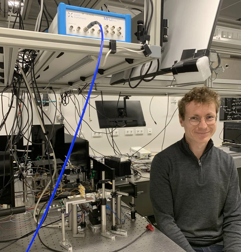
In our recent work [1], we present a robust and portable magnetic field camera based on NV centers in diamond. The sensor is fully fiber‑packaged and chip-integrated. It consists of a 1.4×1.4 mm2 large diamond substrate embedded in a polymer‑on‑silicon platform. Optical fibers interface the diamond substrate’s side facets and define a grid of perpendicularly intersecting green pump and infrared probe laser beams within the substrate, as depicted in Figure 1. The pixels used to measure magnetic fields are located at the beam intersections. Inductor coils on top of each pixel deliver a spin-flipping microwave signal. This frequency-modulated signal is produced by a Rohde & Schwarz SMB100B signal generator that sweeps the signal’s center frequency across the NV centers’ magnetic field-dependent spin resonances. The resulting infrared absorption is measured with a photodiode and demodulated by a Zurich Instruments MFLI Lock‑in Amplifier to infer the per-pixel magnetic field. Switching the pump row and the infrared transmission measurement column allows us to address all pixels and eventually reconstruct a magnetic field image.
Results
We have demonstrated that our camera resolves the magnetic field gradient produced by a current‑driven solenoid placed above one corner of the sensor. The measured field distribution enables precise localization of the coil relative to the device [1]. These results establish that robust, compact, chip‑integrated diamond‑NV sensors can perform magnetic field imaging without moving components or extensive microscope optics.
Outlook
Future work will enhance the camera’s sensitivity and spatial resolution (i.e., pixel count). Envisioned applications include lab‑on‑a‑chip experiments for drug discovery, assessment and optimization of batteries for electromobility, and spaceborne magnetometry.
References
[1] J. M. Bopp et al., ‘Diamond‑on‑chip magnetic field camera for mobile imaging’, Phys. Rev. Applied 23, 034024 (2025)